
Here at Brucom, we believe in investing in our capabilities so that we can offer our clients a full service. That’s why we have our own in-house PCB design and manufacturing facilities equipped with specialist tools to produce high-quality PCBs for a range of applications.
What is a PCB and what is it used for?
A Printed Circuit Board (PCB) is used in almost all electronics for creating electrical connections between different components. It's made of alternating layers of conductive and insulating material. Components can then be added to the board either by mounting to the surface (Surface Mount) or drilling holes through the PCB (Through-hole).
At Brucom, we have the skills, tools and facilities to design and build the PCB to suit our client’s exact use and purpose of the system.
PCB design
The first step in our PCB manufacturing process is to design the PCB. Our engineers assess each customer’s bespoke order, looking at their needs and applications to determine if the system we are going to craft for them would benefit from using a PCB. PCBs are used across many assemblies, and box builds like control panels, safety systems, fuse boxes and more.
If a PCB is required, our engineering team puts together a schematic, visually designing how the PCB will look, function and fit within the system. They design the PCB product carefully considering our client’s uses, applications and installation parameters. As part of this process, our engineers determine what materials, connections and connectors would work best before putting together the initial design.
Once that is done, our engineers create a 3D model of the board to confirm that it will fit into the desired location or is accessible and that there will be no real-world clashes.
To triple-check that the system fits our client’s needs, our engineers order a minimum batch to prototype the design. Once the design is fully checked and signed off, we can then go into full production.
PCB Manufacturing
Once the PCB is designed, we can create a prototype or move on to full-scale manufacturing. To produce a PCB, the boards first go into the screen printer, which uses a stencil to deposit a solder paste onto the component pads.
From there, the boards go through our Pick and Place machine. Once pre-loaded with the relevant components, the machine uses 6 ‘heads’ to pick the components from the pre-loaded feeders and place them onto the pasted pads.
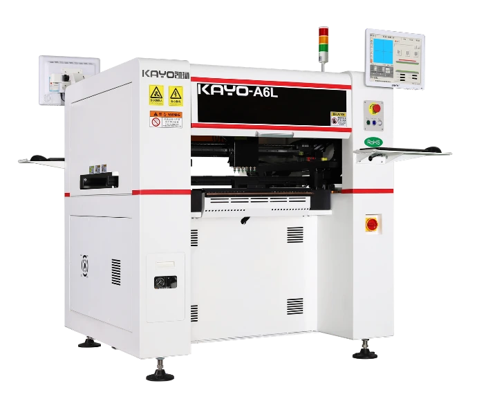
To ensure quality, the boards are inspected for misplaced components before being placed on the reflow oven conveyor. This machine then turns the solder paste into a soldered joint. The boards are inspected again to check they’ve been soldered correctly.
If the board is double-sided and needs components on the other side, they will be placed on the screen printer again. Glue is applied for wave soldering the components, along with any through-hole leaded components. In some cases, the boards have solder paste applied to the second side to be reflowed again, but this only applies where no leaded components require wave soldering.
Once a PCB is built and inspected, we can fit it into the assembly it’s been crafted for. We work with our clients to create full systems fit for their applications. We have expertise crafting a range of box builds and PCB assemblies across multiple industries and applications, specifically the commercial automotive industry.
PCB testing
PCBs are vital systems which often control key functions in an assembly. They must be reliable and work effectively. Our dedicated testing department thoroughly inspects and tests our PCBs before and after they’re added to an assembly.
We take testing seriously, paying careful attention to triple-checking that our products are perfect before despatch. We hold ISO 9001:2015 certification, demonstrating our high standards for quality assurance.
PCB testing methods and tools
All our PCB assemblies are 100% inspected using visual inspection or AOI (automatic optical inspection). We also create specialist test equipment for control panels and PCBs using our in-house PLC control system and software.
By using a PLC to automate all the relevant inputs and monitor for the correct outputs, we are able to simulate the triggers expected in real-world applications, minimising any chance of faulty units leaving our factory.
What is the PLC control system?
PLC (Programmable Logic Controller) devices are programmed by users to trigger other devices under specific conditions.
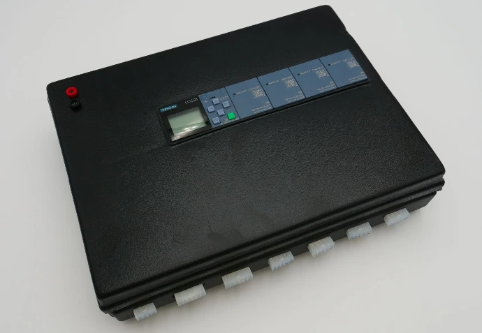
They are widely used for machine automation, safety systems, monitoring stations and even traffic lights. Once programmed, PLCs are extremely versatile and can minimise user input even in the most complex of tasks.
The benefits of PLC testing methods
Previously, all PCB tests used manual switches, LEDs, and buzzers to confirm signals were both sent and received correctly. This process is open to significant human error; a user could miss a step or fail to check a trigger, potentially allowing boards with undetected errors to be sent out.
By implementing PLC as a test method, we can remove the majority of human error by having the PLC control all switching and detection of the PCB. This not only drastically decreases the risk of faulty boards left undetected but also increases efficiency & productivity in our test department while removing the technical knowledge required to test the boards correctly. Once a board is detected by the PLC unit, it follows a pre-set list of triggers, testing each line in sequence with no delay, only stopping when user input is required, for example, flicking a physical switch on the board. If it doesn’t receive the correct signals for each step in the sequence, the unit pauses the test immediately, signalling to the operator that the unit has failed and requires further inspection or manual testing to establish the failure point.
Why we design and manufacture our own PCBs
By bringing the full PCB design and manufacturing process in-house, we can ensure PCB quality remains high. It also allows us to customise the PCB and PCB assembly specifically to our partner’s applications and functionality needs.
At Brucom, our vision is to be a one-stop shop for all commercial automotive needs. We invest in our capabilities so that we can provide everything our customers need, from design to distribution.
Explore our PCB Assembly products
Find out more about the types of PCB we design and manufacture, as well as the PCB assemblies we craft for our clients.
What we offer
Through-hole or surface mount
Programming of PIC & more
Free issue or full turnkey component sourcing